3. The STM32L476 microcontroller
3.1. Introduction
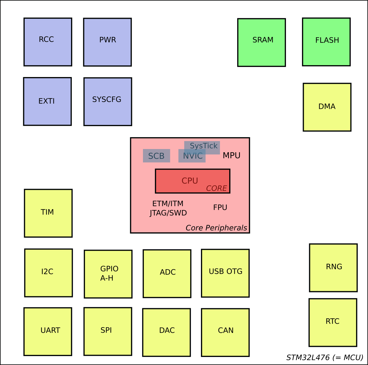
Fig. 3.1.1 Simplified block diagram showing the Cortex M4 core, the core peripherals and the MCU peripherals. The “real” block diagram is shown in the next figure below.
MCU = MiCrocontroller Unit
Power supply 1.71 (!) to 3.6 V.
Cortex-M4 core, max. 80 MHz clock (ca. 100 DMIPS)
Single precision Floating Point Unit (FPU)
Embedded Flash Memory (max. 1 MByte)
64-bit wide
Instruction prefetch queue and branch cache (“ART Accelerator”) to reduce wait states.
Embedded SRAM (overall 128 KByte)
96 Kbyte starting from 0x2000000
32 Kbyte starting from 0x1000000
Memory Protection Unit (MPU)
Additional protected memory regions in Flash and SRAM (“Firewall”)
Low-power modes: 1.1 \(\mu A\), 420 nA, 300 nA, 120 nA, 30 nA.
Timers
Two basic timers (TIM6, TIM7)
Two advanced control timers (TIM1, TIM8)
Up to seven general purpose timers (TIM2, TIM5 || TIM3, TIM4 || TIM15 || TIM16, TIM17)
Low-power timer (LPTIM1, LPTIM2)
Two watchdog timers (IWDG, WWDG)
SysTick timer
Real-time clock powered by VDD or VBAT.
BCD timer/counter, calendar, alarms, wakeup timer (WUT)
32 backup registers for application data (each 32 bit wide)
Interesting new peripherals (compared to STM32VLDiscovery board):
LPUART (Low Power UART)
SAI (Serial Audio Interfaces)
SWPMI (Single Wire Protocol Master Interface)
OPAMP (Operational Amplifier) with programmable gain
Comparator
Touch sensing controller (TSC) for capacitive touch sensing. Supported by STMTouch firmware).
PVD (Programmable voltage detector)
PVM (Peripheral voltage monitoring)
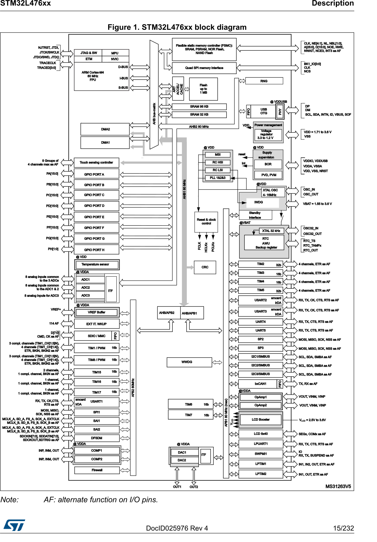
Fig. 3.1.2 Block diagram of the STM32L476 (taken from [L476DS], p. 15).
Package options: LQFP144, LQFP100, LQFP64, UFBGA132, WLCSP81, WLCSP72.
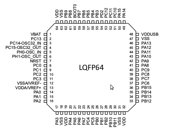
Fig. 3.1.3 STM32L476Rx LQFP64 pinout. This package is used on our Nucleo-64 board.
[L476DS] shows in table 15 (starting from page 60) the pin mappings for all packages.
The AHB bus matrix can connect five masters (columns in Fig. 3.1.4) with seven slaves (rows). Possible interconnections are shown in Fig. 3.1.4 with small circles at crossings.
The ARM Advanced High-performance Bus (AHB) bus is a synchronous 32-bit bus which allows to connect multiple bus masters (e.g. ARM processor and DMA) to multiple slaves (e.g. RAM, external memory interface, AHB/APB bridges). The bus allows (among others) bus-access arbitration, address/data phase, burst-transfer, four transfer-types and wait-states.
Masters:
S0: I-Bus (core fetches instructions)
S1: D-Bus (core fetches data from Flash and SRAM; also used for debugging)
S2: S-Bus (core system bus - used to access data in SRAM and peripherals)
S3: DMA1 (direct memory access)
S4: DMA2 (direct memory access)
Slaves:
Flash I-Code
Flash D-Code
SRAM1
SRAM2
AHB1 peripherals (includeing AHB/APB bridges)
AHB2 peripherals (includeing AHB/APB bridges)
FMC (Flexible Memory Controller) and QSPI (Quad SPI)
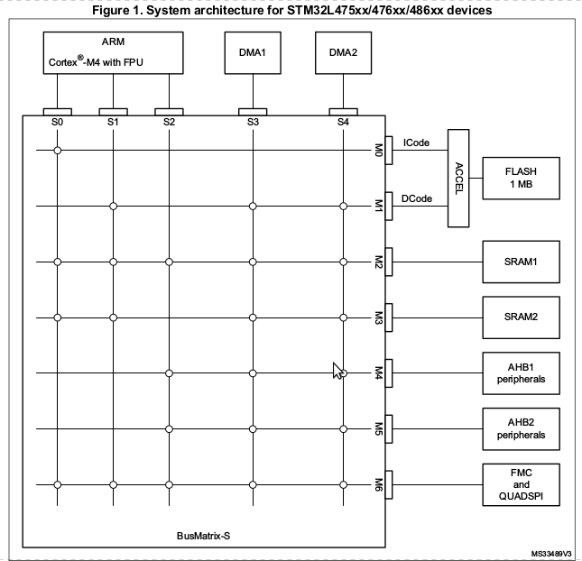
Fig. 3.1.4 STM32L476 bus matrix (taken from [STM32L4RM], ch. 2)
Read chapter 6 about “Memory Systems” in [YIUDG] if you want to know more about this topic.
3.2. Memory Map
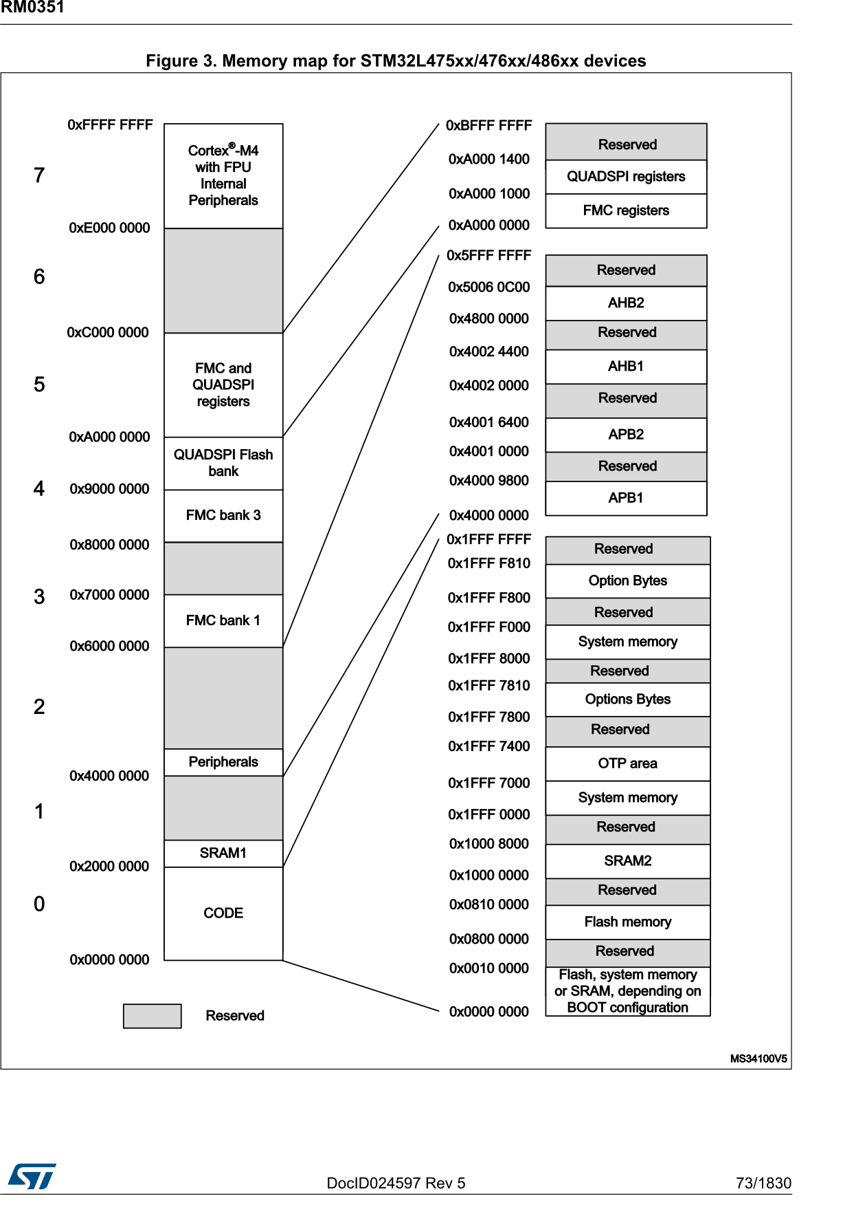
Fig. 3.2.1 Memory Map (taken from [STM32L4RM])
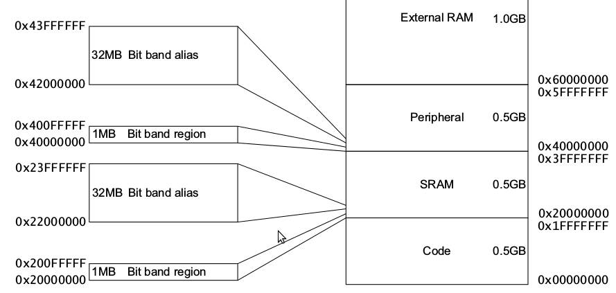
Fig. 3.2.2 Bitband regions in the memory map (taken from [CM4PM])
3.3. Clock generation
See [STM32L4RM], ch. 6, “Reset and Clock Control (RCC)”
Clock sources for the System Clock SYSCLK:
HSI16 (high speed internal - 16 MHz), RC oscillator
MSI (multispeed internal), RC oscillator 100 kHz - 48 MHz
HSE (high speed external), crystal 4 to 48 MHz
PLL clock
After a RESET, the default clock is MSI at 4 MHz.
Additional clock sources:
LSI RC (low speed internal - 32 kHz)
LSE Crystal (low speed external - 32 kHz crystal)
The maximum frequency of the AHB and APB domains is 80 MHz.
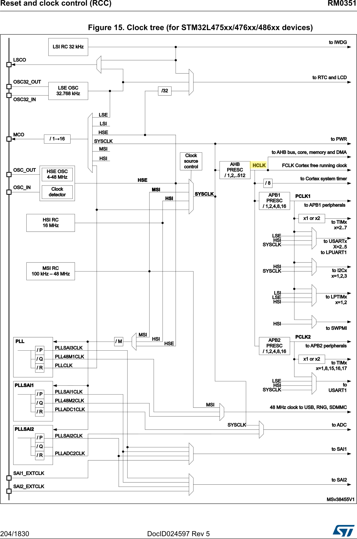
Fig. 3.3.1 STM32L476 clock generation (taken from [STM32L4RM], S. 204)
The HCLK signal is the AHB clock.
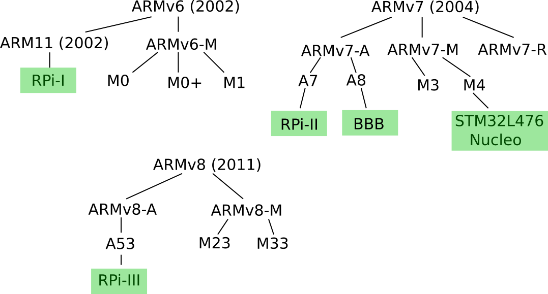
3.4. ARM architectures
3.5. Cortex M4 Core and Core Peripherals
Core = Central Processing Unit (CPU)
RISC: Load/store instructions LDR and STR
“Modified Harvard architecture”: Core has separate instruction and data buses (“I-bus”, “D-bus”), but accesses a unified memory space
No caches
Thumb + Thumb-2 instruction set (no “ARM” instructions)
Single cycle integer DSP Instructions, but no real DSP architecture
Three stage pipelining: fetch, decode, execute
Gate count \(\approx\) 60.000 (+ 25.000 for FPU)
Examples:
MP3 decode at 10-15 MHz clock speed possible
5.1 Dolby digital AC3 headset decode at 50MHz possible
Core + Core-Peripherals:
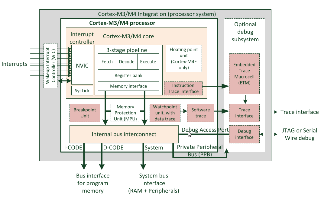
Fig. 3.5.1 Block diagram of Cortex M3 and M4 core (taken from [YIUDG], p. 62). XXX Additional blocks not shown: SCB, Debug (ITM/FPB).
- SCB
System Control Block (also see Sect. 3.10 below).
- SysTick
System Timer
- NVIC
Nested Vectored Interrupt Controller
- FPU
Floating-Point Unit with one, three or 14 cycles (square root, divide).
- MPU
Memory Protection Unit
The registers of the Core Peripherals are described in detail in [CM4PM], chapter 4 (pp. 192-258).
Debug:
- JTAG
Implements the JTAG TAP (Test Access Port), a 20-pin connector.
- SWD
Serial Wire Debug, a 2-wire interface for debugging.
- ITM
Instrumentation Trace Macrocell (ITM) for collecting program execution statistics, data watchpoints, profiling information. The ITM is an application driven trace source that supports printf style debugging to trace OS and application events. It works in combination with the DWT. The ITM gets input from the DWT and The Serial Wire Viewer (SWV) can export a stream of software-generated messages, data trace, and profiling information through a single pin.
- ETM
Embedded Trace Macrocell for high-performance real-time instruction trace capture (optional).
- FPB
Flash Patch and Breakpoint Unit (optional), with up to eight hardware breakpoint comparators that debuggers can use. This unit allows to debug (single step) through code in flash memory.
- DAP
Debug Access Port. Can be implemented as Serial Wire Debug Port (SW-DP) or Serial Wire JTAG Debug Port (SWJ-DP). The SWJ-DP can operate in JTAG mode (after power on) and can be switched to Serial Wire mode later.
- DWT
Data Watchpoint and Trace. Collects instruction execution statistics: Compares data address, program counter, triggers PC sampler events, data address sampler events.
- SWV
Serial Wire Viewer. Emit trace data from ETM or ITM over a single wire to external trace analyzer units.
3.6. Modes of operation
Two access levels for code: privileged, unprivileged. Bit 0 in CONTROL register selects access level for thread mode.
Two modes: thread (from reset / privileged and unprivileged), handler (during exception / privileged).
Two operating states: thumb, debug
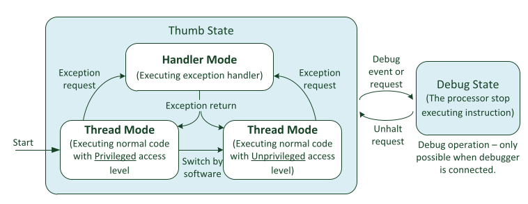
Debugging in halt mode or debug monitor mode.
3.7. Booting
Boot modes selectable by BOOT0 and BOOT1 pins. Boot sources are (a) system memory, (b) Flash, (c) SRAM.
BOOT1  BOOT0
  X      0     boot from main flash memory
  0      1     system memory
  1      1     embedded SRAM
BOOT0 is connected to CN7, pin 7 of the STM32L476 Nucleo board.
The BOOT1 can be set via bit 23 (nBOOT1) in the User and read protection option bytes register (0x1FFF7800). See section 3.4 FLASH option bytes in [STM32L4RM] (p. 108). Important: “BOOT1 is the opposite of the nBOOT1 option bit”.
Booting from system memory means, that a bootloader code is executed from Flash memory. The bootloader code is secured from write and erase operations. It allows to write the user flash memory and the SRAM from various sources: UART, SPI, I2C, USB (DFU) or CAN.
Reset Sequence
Get starting value for R13 (stack pointer, MSP) from address 0x00000000. The initial stack pointer value should be set to the first memory location after the top of stack. The reason is, that a push operation first decrements the stack pointer and then stores the value. This is called a full descending stack.
Get reset vector from address 0x00000004. This is the starting address of program execution.
3.8. Register
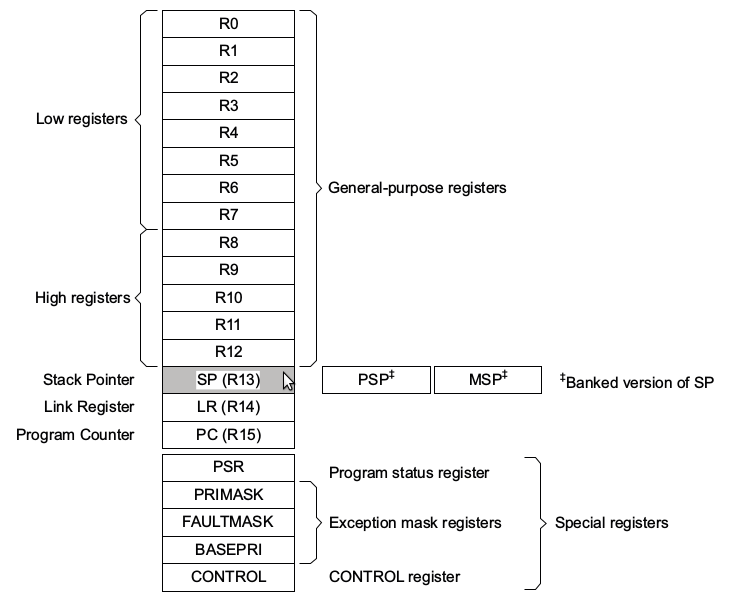
- R0-R12
General-purpose registers
- SP (R13)
Stack Pointer. MSP = Main Stack Pointer (after Reset). PSP = Process Stack Pointer.
CONTROL[1] = 0 selects MSP (default stack)
CONTROL[1] = 1 selects PSP (alternate stack)
- LR (R14)
Link Register. It stores the return information for subroutines, function calls, and exceptions. On reset, the processor sets the LR value to 0xFFFFFFFF.
- PC (R15)
Program Counter. The Program Counter (PC) is register R15. It contains the current program address. On reset, the processor loads the PC with the value of the reset vector, which is at address 0x00000004 . Bit[0] of the value is loaded into the EPSR T-bit at reset and must be 1.
- PSR
Program Status Register. Contains APSR, IPSR and EPSR.
APSR - Application Program Status Register
IPSR - Interrupt Program Status Register. The IPSR contains the exception type number of the current Interrupt Service Routine (ISR).
EPSR - Execution Program Status Register
- PRIMASK
Priority Mask Register. The PRIMASK register prevents activation of all exceptions with configurable priority. Only PRIMASK[0] ist used.
- FAULTMASK
Fault Mask Register. The FAULTMASK register prevents activation of all exceptions except for Non-Maskable Interrupt (NMI). Only FAULTMASK[0] is used.
- BASEPRI
Base Priority Mask Register. All exceptions with priority >= BASEPRI[7:0] are disabled.
- CONTROL
CONTROL register. The CONTROL register controls the stack used and the privilege level for software execution when the processor is in Thread mode and, if implemented, indicates whether the FPU state is active.
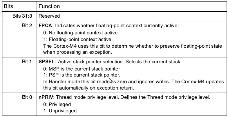
Fig. 3.8.2 CONTROL register bit definitions (taken from [CM4PM], p. 24)
The special registers can only be accessed with MSR and MRS assembler instructions:
MRS  <reg>, <special_reg>      @ read from special register
MSR  <special_reg>, <reg>      @ write to special register
3.9. Status Register
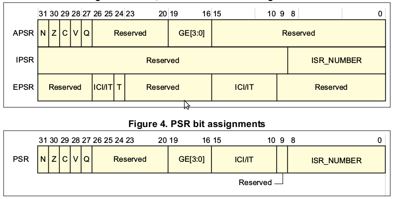
- N
Negative flag
- Z
Zero flag
- C
Carry or borrow flag
- V
Overflow flag
- Q
DSP overflow and saturation flag
- GE
APSR[19:16] Greater than or equal flags (GE[3:0])
By using the self-written flags function in GDB you can print the
contents of the status register in a human readable form (see section
about GDB debugging below):
(arm-gdb) flags
N=0 Z=0 C=1 V=0 Q=0 GE=0 ICI/IT=0x0 Exc#=56
3.10. System Exceptions and Interrupts
HardFault, MemManage fault, UsageFault, and BusFault are fault exceptions handled by the fault handlers.
NMI, PendSV, SVCall SysTick, and the fault exceptions are all system exceptions that are handled by system handlers.
The IRQ interrupts are the exceptions handled by Interrupt Service Routines (ISRs).
The interrupt priority is given by an 8-bit number, smaller numbers have higher priority:
-3
     RESET
-2
     NMI
-1
     Hard fault
 0, 16, 32, 48, 64, ..., 240
     System exceptions (upper 4 bits only). Defaults to zero.
 0, 16, 32, 48, 64, ..., 240
     IRQ (set in the NVIC)
The priority level for the exception handlers with configurable priority is set by the SHPRx registers (SHPR1, SHPR2, SHPR3), which are located in the System Control Block (SCB). Each priority value is stored in the upper four bits of an 8 bit wide field, the lower 4 bits are zero. The number of bits depend on the implementation. The same bit organization holds for the 8-bit prio values in the NVIC_IPR59 – NVIC_IPR0 registers (see Sect. 3.10.4).
After reset, all these exceptions (”system handlers”) have priority 0 (highest).
The SHCSR register (system handler control and state register) in the SCB enables/disables the system handlers and indicates the pending/active status.
Priority groups: The priority number can optionally be split into a group priority and a subpriority field (see SCB->AIRCR register).
The system handlers are controlled by the SCB registers:
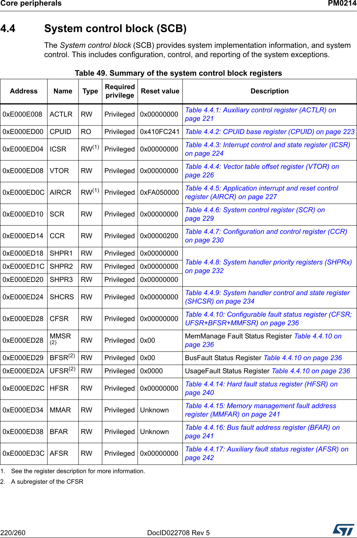
Fig. 3.10.1 System Control Block registers (taken from [CM4PM], ch. 4 “System control block”)
All registers in the SCB can only be accessed in the privileged level.
3.10.1. Exception Vectors
Nummer |
IRQ Nr |
Type |
Priority |
Vector Addr |
Enable |
Activation |
|---|---|---|---|---|---|---|
1 |
– |
Reset |
-3 |
0x00000004 |
Always |
Async |
2 |
-14 |
NMI |
-2 |
0x00000008 |
Always |
Async |
3 |
-13 |
Hard fault |
-1 |
0x0000000C |
Always |
– |
4 |
-12 |
MemManage fault |
Programmable (SHPR1) |
0x00000010 |
NVIC SHCSR 0xE000ED24, bit 16 |
Sync |
5 |
-11 |
BusFault |
Programmable (SHPR1) |
0x00000014 |
NVIC SHCSR 0xE000ED24, bit 17 |
Sync (precise), async (imprecise) |
6 |
-10 |
UsageFault |
Programmable (SHPR1) |
0x00000018 |
NVIC SHCSR 0xE000ED24, bit 17 |
Sync |
7 – 10 |
– |
Reserved |
– |
– |
– |
– |
11 |
-5 |
SVCall |
Programmable (SHPR2) |
0x0000002C |
Always |
Sync |
12 – 13 |
– |
Reserved |
– |
– |
– |
– |
14 |
-2 |
PendSV |
Programmable (SHPR3) |
0x00000038 |
Always |
Async |
15 |
-1 |
SysTick |
Programmable (SHPR3) |
0x0000003C |
SYST_CSR (0xE000E010), bit 0 |
Async |
16 |
0 |
IRQ0 |
Programmable (0xE000E400) |
0x00000040 |
NVIC SETEN (0xE000E100) |
Async |
17 |
1 |
IRQ1 |
… |
… |
… |
… |
18 |
… |
… |
… |
… |
… |
… |
The STM32L476 has 82 maskable interrupt channels IRQ0 - IRQ81 (see Sect. 3.10.4).
3.10.2. Enable/disable interrupt processing
“Change Processor State” instruction (CPS). The “i” is for PRIMASK, the “f” is for FAULTMASK. The comments contain the equivalent CMSIS intrinsic functions. ):
# Disable interrupts and configurable fault handlers (set PRIMASK)
CPSID i      # void _disable_irq(void)
# Enable interrupts and configurable fault handlers (clear PRIMASK)
CPSIE i      # void _enable_irq(void)

# Disable interrupts and all fault handlers (set FAULTMASK)
CPSID f
# Enable interrupts and all fault handlers (clear FAULTMASK)
CPSIE f
CMSIS API
_set_BASEPRI(prio)              // shift prio argument
NVIC_SetPriority(IRQn, prio)    // don't shift prio argument
3.10.3. Interrupt behavior
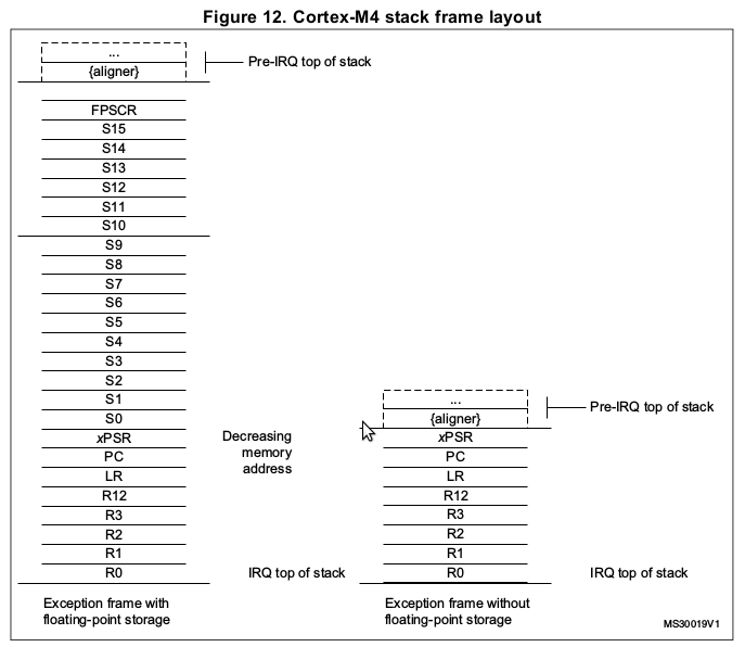
“Stacking”
Cortex-M4 stack frame layout for non-floating-point state.
   old SP (N) ---->
                    xPSR
                    PC
                    LR
                    R12
                    R3
                    R2
                    R1
new SP (N-32) ----> R0
“Caller saved” registers according to ARM Architecture Procedure Call Standard: R0-R3, R12, LR, PC, PSR.
See Sect. 3.12 for the stack frame layout with FPU.
Vector fetch
Register updates
Either MSP or PSP will be updated to the new location during stacking. During ISR execution, the MSP will be used if the stack is accessed.
The IPSR will be updated to the new exception number.
The PC changes to the vector handler.
The LR will be updated to EXC_RETURN.
EXC_RETURN[31:5] all set to 1.
EXC_RETURN[4:0] defines how the return will work: to handler/thread mode, fp- or non-fp state, return to MSP/PSP. Details are in [CM4PM], p. 43.
Exception Exit
a.k.a. “exception return”, “interrupt return”
Special value stored in LR (EXC_RETURN) is used
Trigger exception return with one of (a), (b) or (c)
(a)   BX <reg>      ; EXC_RETURN must still be in LR

(b)   POP {PC}      ; LR was pushed on stack after handler starts

(c)   LDR, or LDM   ; PC as destination register
Note that this is a “normal” return instruction as used by an ordinary function call return. The interrupt handler can thus be implemented as a C function.
On exception return is carried out
unstacking (registers are restored from stack; stack pointer is changed back)
NVIC register update:
Active bit of the exception is cleared
If an external interrupt is still asserted, the pending bit will be set again
3.10.4. NVIC
Core peripheral
The STM32L476 has 82 maskable interrupt channels.
16 programmable priority levels (4-bit).
The number of bits for the priority levels depend on the implementation (e.g. 3 bit for Tiva Cortex-M4, 4 bit for STM32F4), use CMSIS macro
__NVIC_PRIO_BITSto find out the actual number of bits. These are the upper 3 or 4 bits of the 8-bit NVIC prio configuration registers.The NVIC supports priority grouping. This divides each interrupt priority register into an upper part preempt priority (or group priority) and a lower part subpriority. The preempt priority level determines if one interrupt can preempt another. The subpriority level is used when exceptions with the same preempt priority are pending. It is best to not use priority grouping by calling
NVIC_SetPriorityGrouping(0U).CMSIS functions:
void NVIC_SetPriorityGrouping(uint32_t priority_grouping) Set the priority grouping
void NVIC_EnableIRQ(IRQn_Type IRQn)        Enables an interrupt or exception.
void NVIC_DisableIRQ(IRQn_Type IRQn)       Disables an interrupt or exception.
void NVIC_SetPendingIRQ(IRQn_Type IRQn)    Sets the pending status of interrupt or exception to 1.
void NVIC_ClearPendingIRQ(IRQn_Type IRQn)  Clears the pending status of interrupt or exception to 0.
uint32_t NVIC_GetPendingIRQ(IRQn_Type IRQn) Reads the pending status of interrupt or exception.
uint32_t NVIC_GetActive (IRQn_t IRQn) Return the IRQ number of the active interrupt

void NVIC_SetPriority(IRQn_Type IRQn, uint32_t priority)
                                            Sets the priority of an interrupt or exception with configurable priority level to 1.
uint32_t NVIC_GetPriority(IRQn_Type IRQn)   Reads the priority of an interrupt or exception with configurable priority level.
void NVIC_SystemReset (void)                Reset the system
The IRQn argument is 0 for the IRQ0 (vector address 0x40).
NVIC configuration registers:
NVIC_ISER0 - NVIC_ISER7     Interrupt set-enable registers (8 x 32-bit)
NVIC_ICER0 - NVIC_ICER7     Interrupt clear-enable registers (8 x 32-bit)
NVIC_ISPR0 - NVIC_ISPR7     Interrupt set-pending registers (8 x 32-bit)
NVIC_ICPR0 - NVIC_ICPR7     Interrupt clear-pending registers (8 x 32-bit)
NVIC_IABR0 - NVIC_IABR7     Interrupt active bit registers (8 x 32-bit)
NVIC_IPR0  - NVIC_IPR59     Interrupt priority registers (60 x 32-bit)
                            PRI_239...PRI_0
STIR                        Software Trigger Interrupt Register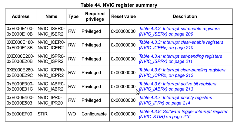
STM32 interrupts are both level sensitive and pulse sensitive (= edge-triggered interrupts).
Some interrupts (taken from [STM32L4RM], ch. 13: “NVIC”):
IRQNr  Short      Long                          Vector Address
0      WWDG       Window Watchdog               0040
...
6      EXTI0      EXTI Line0 interrupt          0058
7      EXTI1      EXTI Line1 interrupt          005C
8      EXTI2      EXTI Line2 interrupt          0060
9      EXTI3      EXTI Line3 interrupt          0064
10     EXTI4      EXTI Line4 interrupt          0084
...
18     ADC1_2     ADC1 and ADC2 interrupt       0088
...
23     EXTI9_5    EXTI Line[9:5] interrupts     009C
...
37     USART1     USART1 global interrupt       00D4
38     USART2     USART2 global interrupt       00D8
...
40     EXTI15_10  EXTI Line[15:10] interrupts   00E0
...
52     UART4      UART4 global interrupt        0110
...
80     RNG        RNG global interrupt          0180
81     FPU        Floating point interrupt      0184
The NVIC also implements the SysTick timer (see Sect. 3.10.6 below).
3.10.5. EXTI
(see [STM32L4RM], ch. 14)
Not a core peripheral.
EXTended Interrupts and events controller.
Generation of up to 40 event/interrupt requests EXTI0-39. All events can wake up from Stop 0 and Stop 1 modes. Some events can wake up from Stop 2 mode.
26 configurable lines
Interrupt selection: look at EXTI_IMR, EXTI_RTSR, EXTI_FTSR. Configure NVIC IRQ channel mapped to EXTI.
14 direct lines
Interrupt selection: No EXTI configuration.
The GPIO pins can be routed over 16 multiplexers to the EXTI0-15 lines. Each of the multiplexers has 8 to 9 inputs. The bits to select the multiplexer inputs are contained in the System Configuration Controller SYSCFG ([STM32L4RM], chapter 9), registers SYSCFG_EXTICR1, SYSCFG_EXTICR2, SYSCFG_EXTICR3, SYSCFG_EXTICR4.
EXTI lines (taken from [STM32L4RM], ch. 14)
EXTI line         Line source              Line type
------------------------------------------------------------
0-15              GPIO                          conf
16                PVD                           conf
17                OTG FS wakeup event           direct
18                RTC alarms                    conf
19                RTC tamper/timestamp/CSS_LSE  conf
20                RTC wakeup timer              conf
21                COMP1 output                  conf
22                COMP2 output                  conf
23                I2C1 wakeup                   direct
24                I2C2 wakeup                   direct
25                I2C3 wakeup                   direct
26                USART1 wakeup                 direct
27                USART2 wakeup                 direct
28                USART3 wakeup                 direct
29                USART4 wakeup                 direct
30                USART5 wakeup                 direct
31                LPUART1 wakeup                direct
32                LPTIM1                        direct
33                LPTIM2                        direct
34                SWPMI1 wakeup                 direct
35                PVM1 wakeup                   conf
36                PVM2 wakeup                   conf
37                PVM3 wakeup                   conf
38                PVM4 wakeup                   conf
39                LCD wakeup                    direct
Registers
EXTI_IMR1   Interrupt Mask Register 1
EXTI_EMR1   Event Mask Register 1
EXTI_RTSR1  Rising Trigger Selection Register 1
EXTI_FTSR1  Falling Trigger Selection Register 1
EXTI_SWIER1 Software Interrupt Event Register 1
EXTI_PR1    Pending register 1
EXTI_IMR2   Interrupt Mask Register 2
EXTI_EMR2   Event Mask Register 2
EXTI_RTSR2  Rising Trigger Selection Register 2
EXTI_FTSR2  Falling Trigger Selection Register 2
EXTI_SWIER2 Software Interrupt Event Register 2
EXTI_PR2    Pending Register 2
Block diagram (taken from [STM32L4RM], ch. 14: “EXTI”)
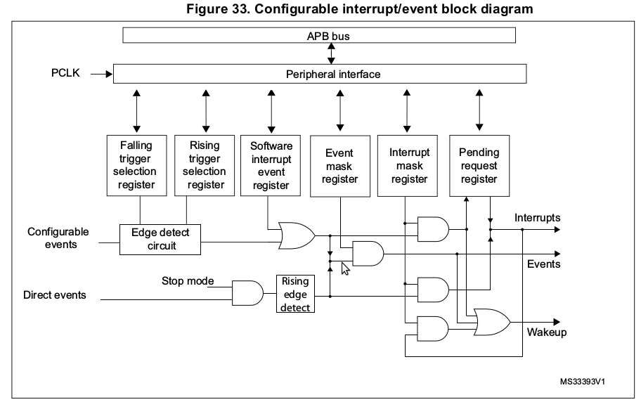
Fig. 3.10.3 Configurable interrupt/event block diagram
External GPIO pin to EXTI mapping (taken from [STM32L4RM], ch. 14: “EXTI”). The SYSCFG_EXTICR1 to SYSCFG_EXTICR4 registers are located in the System Configuration Controller (SYSCFG), see [STM32L4RM], ch. 9.
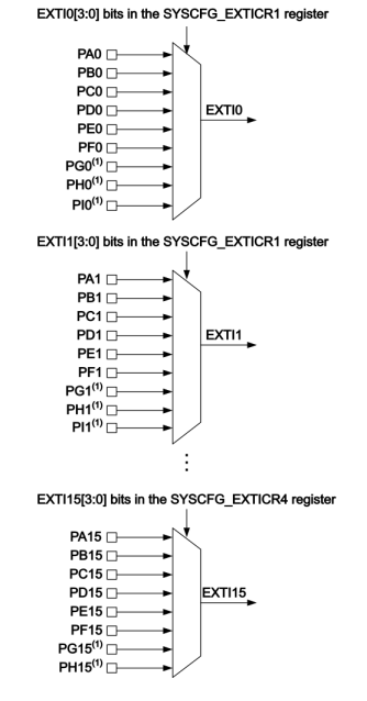
Fig. 3.10.4 GPIO pin to EXTI mapping
3.10.6. SysTick
The processor has a 24-bit system timer, SysTick, that counts down from the reload value to zero, reloads (wraps to) the value in the STK_LOAD register on the next clock edge, then counts down on subsequent clocks.
When the processor is halted for debugging the counter does not decrement.
System handler #15.
Implemented in the NVIC.
Registers
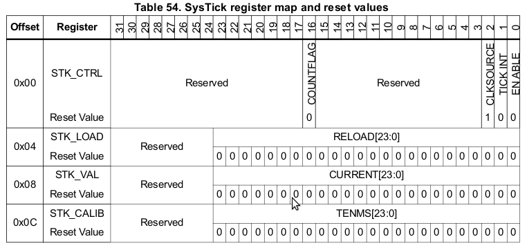
Fig. 3.10.5 Systick registers
CMSIS definitions are in
CMSIS/Include/core_cm4.h.
3.11. GPIO
Lit.: [STM32L4RM], ch. 8: General-purpose I/Os (GPIO)
Ports A-I, each 16 bit
Each port has
Four configuration registers: GPIOx_MODER, GPIOx_OTYPER, GPIOx_OSPEEDR and GPIOx_PUPDR
Two data registers: GPIOx_IDR and GPIOx_ODR
A set-reset register: GPIOx_BSRR
A locking-register: GPIOx_LCKR
Two alternate-function registers: GPIOx_AFRH and GPIOx_AFRL
GPIO configuration registers
GPIOx_MODER    GPIO port mode register,  x=A-I
GPIOx_OTYPER   GPIO port output type register
GPIOx_OSPEEDR  GPIO port output speed register
GPIOx_PUPDR    GPIO port pull-up/pull-down register
GPIOx_IDR      GPIO port input data register
GPIOx_ODR      GPIO port output data register
GPIOx_BSRR     GPIO port bit set/reset register
GPIOx_LCKR     GPIO port configuration lock register
GPIOx_AFRL     GPIO alternate function low register
GPIOx_AFRH     GPIO alternate function high register
GPIOx_BRR      GPIO port bit reset register
GPIOx_ASCR     GPIO port analog switch control register
Each port pin can have up to 16 different alternate functions. See the registers GPIOx_AFRL and GPIOx_AFRH.
The “alternate function mapping” table is in the datasheet, see [AFTABLE].
Compare the table with the LQFP64 pinout in Fig. 3.1.3.
Each of the GPIO port pins can be configured as
Input floating
Input pull-up
Input-pull-down
Analog
Output open-drain with pull-up or pull-down capability
Output push-pull with pull-up or pull-down capability
Alternate function push-pull with pull-up or pull-down capability
Alternate function open-drain with pull-up or pull-down capability
3.12. FPU
Register
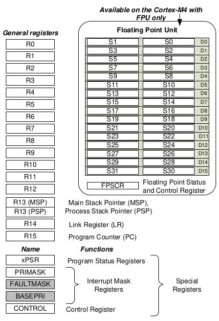
Fig. 3.12.1 Cortex M4 Core Registers with FPU (taken from the Whitepaper “Cortex-M for beginners” by Joseph Yiu)
Floating Point Unit (IEEE 754)
single precision add, subtract, multiply, divide, mac, sqrt
32 32-bit registers: S0 … S31. The registers S0 … S15 are caller saved.
SCB->CPACR, FPU->FPCCR, FPU->FPCAR, FPU->FPDSCR, FPU->FPSCR
5 exceptions: see the exception flags in FPSCR.
Typical instructions (cycles are in braces): VADD.F32 (1), VMUL.F32 (1), VDIV.F32 (14), VSQRTF.F32 (14)
src/startup_stm32l476xx.s:.fpu fpv4-sp-d16 <-- FPU .fpu softvfp <-- Software
Compiler options:
-mfloat-abi=hard -mfpu=fpv4-sp-d16 -ffast-math
Stacking frame layout for exceptions with FPU:
Float representation (only single precision supported in STM32L476)
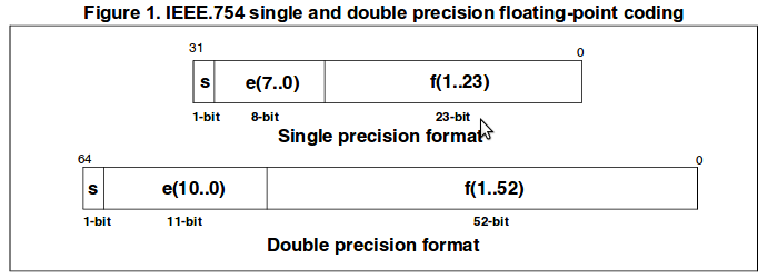
Fig. 3.12.3 (taken from AN4044)
Lit.:
[CM4PM], ch. 4.6, “Floating point unit”
Floating point unit demonstration on STM32 microcontrollers, AN4044, ST micro 2016 (with Julia- and Mandelbrot-Set demos).